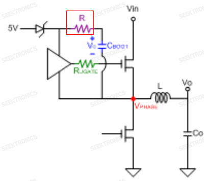
In the peripheral circuit design of DC-DC BUCK chips, we usually add capacitors or a combination of capacitors + resistors between the BOOT and SW pins, this piece of circuit is called bootstrap circuit, the capacitors and resistors in the bootstrap circuit are called bootstrap capacitors and bootstrap resistors.
What is a bootstrap capacitor?
DCDC Buck chip has a pin called BOOT, and some are called BST. The following is an explanation of the BOOT pin of a DCDC chip. In the external circuit design, a capacitor, generally 0.1uF, is needed between the BOOT and SW pin, and is connected to the driver end of the high-end MOS tube of DCDC.
How does a bootstrap capacitor work?
The following is a block diagram of a DCDC BUCK chip, the top NMOS is called the high-side MOSFET and the bottom NMOS is called the low-side MOSFET.
When the high side MOS tube is turned on, SW is VIN, SW charges and stores energy in the inductor, and the inductor current is rising; when the low side MOS tube is turned on, SW is GND, and at this time the inductor supplies power to the load through the renewal diode.
This is the general principle of the DC-DC BUCK.
If this C is not added, then when Vgs<Vgs(th), there will be a high-side MOS tube that cannot be turned on; after adding C, using the characteristic that the capacitor voltage cannot change suddenly, when SW becomes VIN, then the voltage on BOOT will rise to VIN+5V, at this time Vgs will be greater than Vgs(th), and the high-side MOS tube will be turned on.
How do choose the right voltage rating of the bootstrap capacitor?
Generally the maximum value of BOOT to SW is given on SPEC, which is 6.5V as shown below, so generally a capacitor with 10V/16V withstand voltage value can be selected.
Bootstrap resistor selection
In fact, in the bootstrap circuit, you can also add a resistor, generally called BOOT resistor. the role of the BOOT capacitor is that when the SW is at a high level, the use of the voltage across the capacitor can not be a sudden change in characteristics, will pump the BOOT pin voltage to a higher voltage than the SW, maintaining the high side MOSFET on state.
The addition of the BOOT resistor, and the BOOT capacitor forms the RC charging circuit.
The size of the BOOT resistor determines the switching speed of the high-edge MOSFET. Generally, the higher the Boot resistance is, the slower the high-edge MOSFET will open. At this time, the smaller the peak on SW, and the better the EMI characteristics will be. The smaller the Boot resistance, the faster the MOSFET opens, the larger the spikes on the SW, so sometimes the SW will reserve RC to ground absorption.


Comments
Post a Comment