1. The gate
1.1 AND gate
And gate is two inputs and one output, when both inputs are 1, the output will be 1, otherwise the output will be 0. The underlying principle of the gate is explained by relays as follows:

In the case of an energized coil, there will be a magnetic effect. In the figure above we can see that if the two coils are energized, they will each suck down the switch above them, thus making the switch closed, which will then eventually lead to the bulb being energized.
We can see that there is a power supply connected to the bulb, and there are two switches on this circuit, which are controlled by the other two power supplies, so three power supplies are used in the whole circuit.

After simplifying the circuit, it looks like this above. As you can see, the light bulb should have the power to ignore, leaving only two switching power supplies.
1.2 Or-gate
OR-gate also has two inputs and one output. If at least one of the two inputs is 1, then the output is 1..
.jpg)
or-gate is composed of four power supply, two power supply is directly connected to the bulb, the other two power supply is connected to the relay, and each relay control a bulb power switch

1.3 Not-gate
The not-gate represents the opposite of the output and the input, if the input is 1, then the output is 0, if the input is 0, then the output is 1.

Not the door is the relay power closed, the light bulb power pull down, and then the light bulb power off; if the relay power off, the light bulb power pop up and then closed.

1.4 Exclusive-OR gate
The above AND gate,Or-gate and Not-gates is the most basic gate circuit. We can combine with or without gate to generate new gate circuits, such as the Exclusive-OR gate we are talking about. Exclusive-OR gate means that the output is 1 when the two inputs are different, and 0 when the two inputs are the same.

2. Adder
If you have studied computer principles, you know that the main calculation unit of early computers is the adder, that is to say, subtraction, multiplication, and division can be done with the adder, so how to assemble an adder through the gate circuit we mentioned above?
We know that the underlying computer does its logical computations in binary, so the adder we need to complete is also to implement binary addition. Binary addition has the following scenarios: 0+0=0, 0+1=1, 1+1=10. Can you see any signs? The output is 0 when the two values are the same, and 1 when the two values are different. Yes, it is the property of the Exclusive-OR gate that we talked about above.
When it comes to addition, there is rounding, and for binary, there is only rounding if both inputs are 1. And this property just fits the And gate we talked about above. Therefore, the sum of binary can be achieved by an Exclusive-OR gate, and the feed can be achieved by a And gate, and the combination of the two can complete the addition of two binary operations. (The circuit can be called a half-adder)
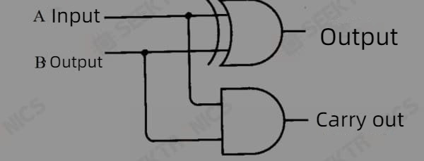
The following is by drawing the circuit of the half adder at the relay level, you can see how the most basic circuit is to implement the adder, which may also be many students at the beginning of the computer are puzzled: how the circuit is to achieve the current computer so complex calculations. This is the most basic principle of implementation.

A half adder is a device to achieve the addition of two one-bit binary numbers, the above figure can be simplified to a half-adder if you consider the input, which you can achieve this by combining two half adders, the following figure

3. Flip-flop
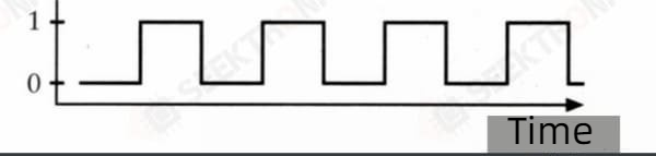
3.1 Oscillators
Relays can implement gate circuits. Here we will look at one more flirty circuit implemented by relays.

We see this circuit above, the circuit is turned on so that the electromagnet pulls the metal reed down, when the metal reed changes position, the circuit is no longer complete, the electromagnet loses its magnetism and the metal reed pops back to its original position.
The output of the circuit is the change between providing voltage and not providing voltage, and this circuit is called an oscillator. It is also known as a clock
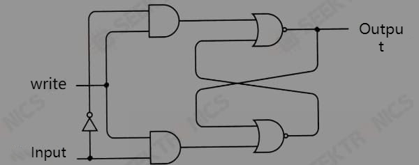
3.2 R-S Flip-flop
.jpg)
This circuit has the following characteristics:
Closing the switch above makes the light bulb light, and when it is disconnected again, the light bulb is still on.
Closing the switch below makes the light bulb go out, and when it is disconnected again, the light bulb is still off.
The peculiar thing about circuits is that sometimes when both switches are off, the bulb is on; and sometimes, when both switches are off, the bulb is not on. When both switches are off, the circuit has two steady states, and such a circuit is called a flip-flop.
This circuit remembers which switch was last closed first. This type of trigger is called an R-S (Reset-Set) trigger.
3.3 D-type latches
.jpg)
This circuit is called a level-triggered D-type flip-flop, with D representing the data-side input. Level triggering means that the flip-flop saves the input value of the data side only when the hold bit input is a specific level ("1" in this case). It can also be called 1-bit memory.
4. Memory
4.1 Memory principle
This is the same flip-flop, but now the Q output is named input-output and the clock input is named as a write-in. The circuit is also called a latch.
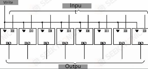
8 such latches connected together is 8 for input and output.
What if one output is selected out of 8? Look at the following figure, which is an 8-1 selector
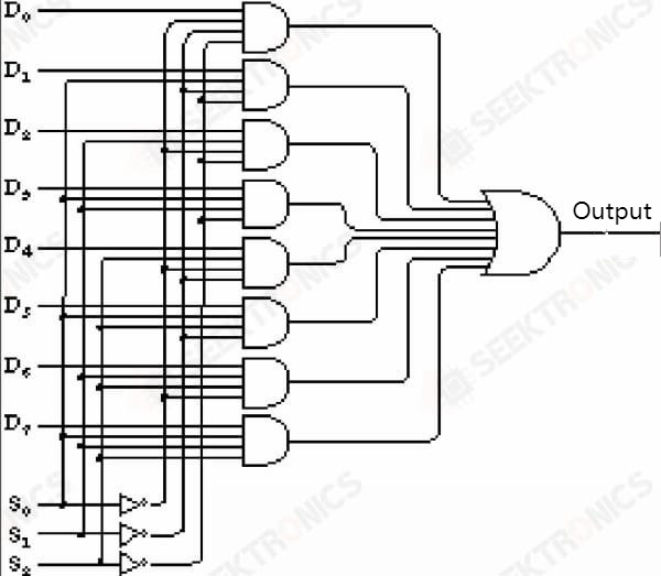
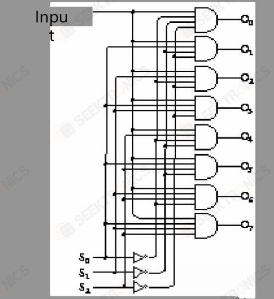
The following one is a 3-8 decoder
The complete circuit of the 8 latches is as follows
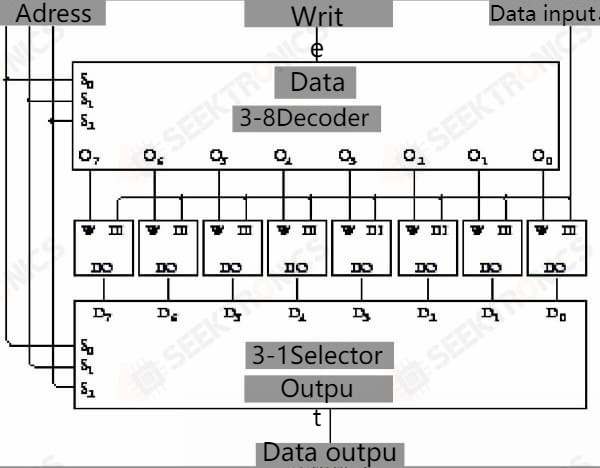
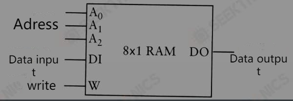
A simplified diagram is as follows.
4.2 Large Memory Implementation Principle
As we saw in the previous section that there are many lines for an 8-bit capacity latch. But in real computers, we have memory in G. If we follow the method described in the previous section to extend out the real available physical memory, the line complexity is more than human imagination.
To solve the problem of wiring large memories, engineers came up with the matrix approach, which means placing one latch after another in the form of a matrix, as shown in the figure below:

In the above figure, the latch can be selected only if the horizontal address line and the vert al address line are 1, and then look at the write and read signals to decide whether it can be written or read.
To abstract the memory layout, we can represent it by the following diagram

As described above, an address can only write or read 1 bit of data. What if you want to write or read 1 byte of data at the same time, that is, 8 bits? Very simple, the address line at the same time with 8 memory like the above line, as shown below:

4.3 Real Physical Memory Modules
The memory has a capacity of 1M, by gradually enlarging the memory, we look at the process of realization.

One of the little black bars is enlarged to look like this:

One of the little squares is enlarged to look like this:

Each square is enlarged as follows:

Comments
Post a Comment